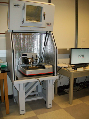
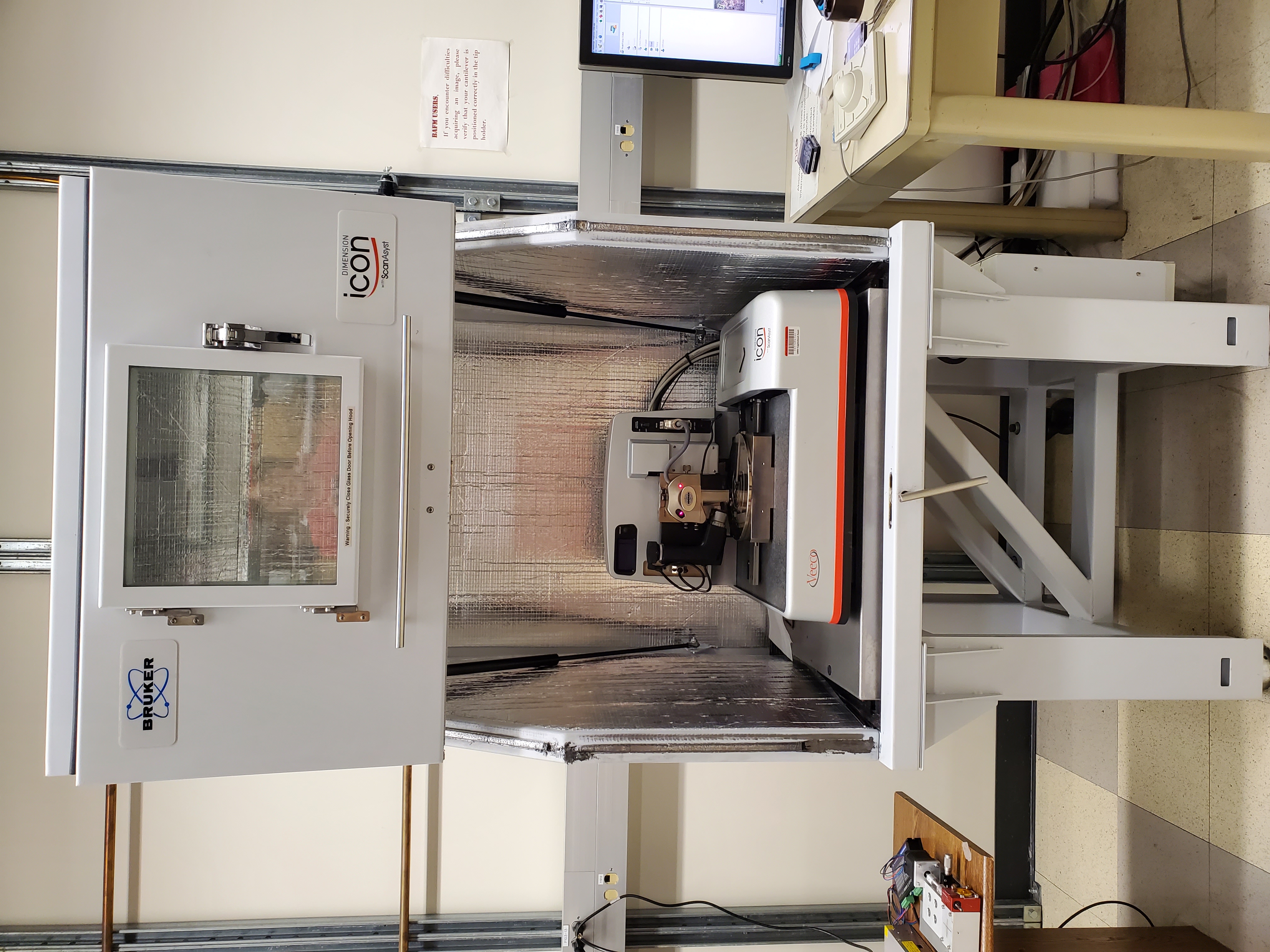
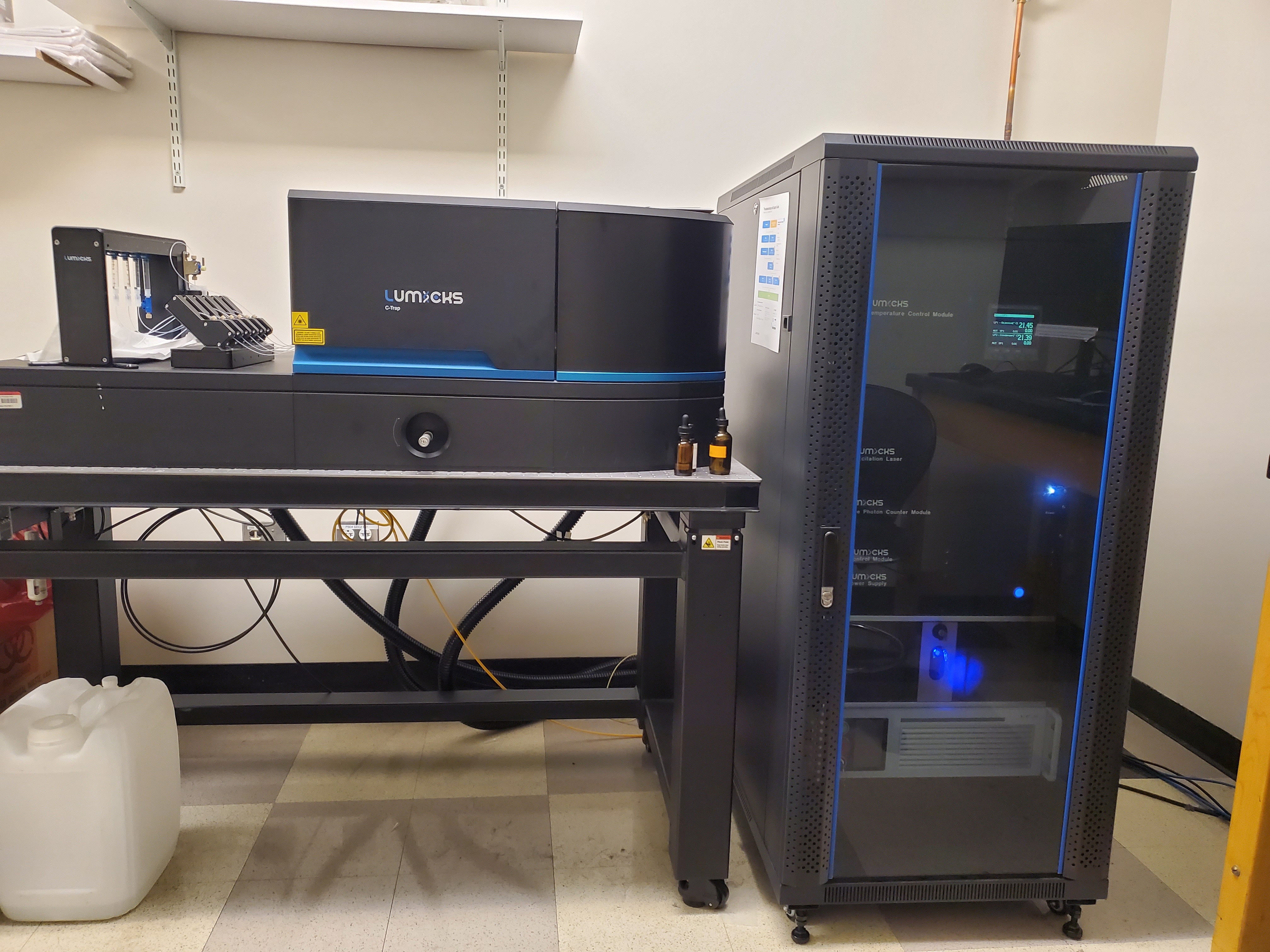
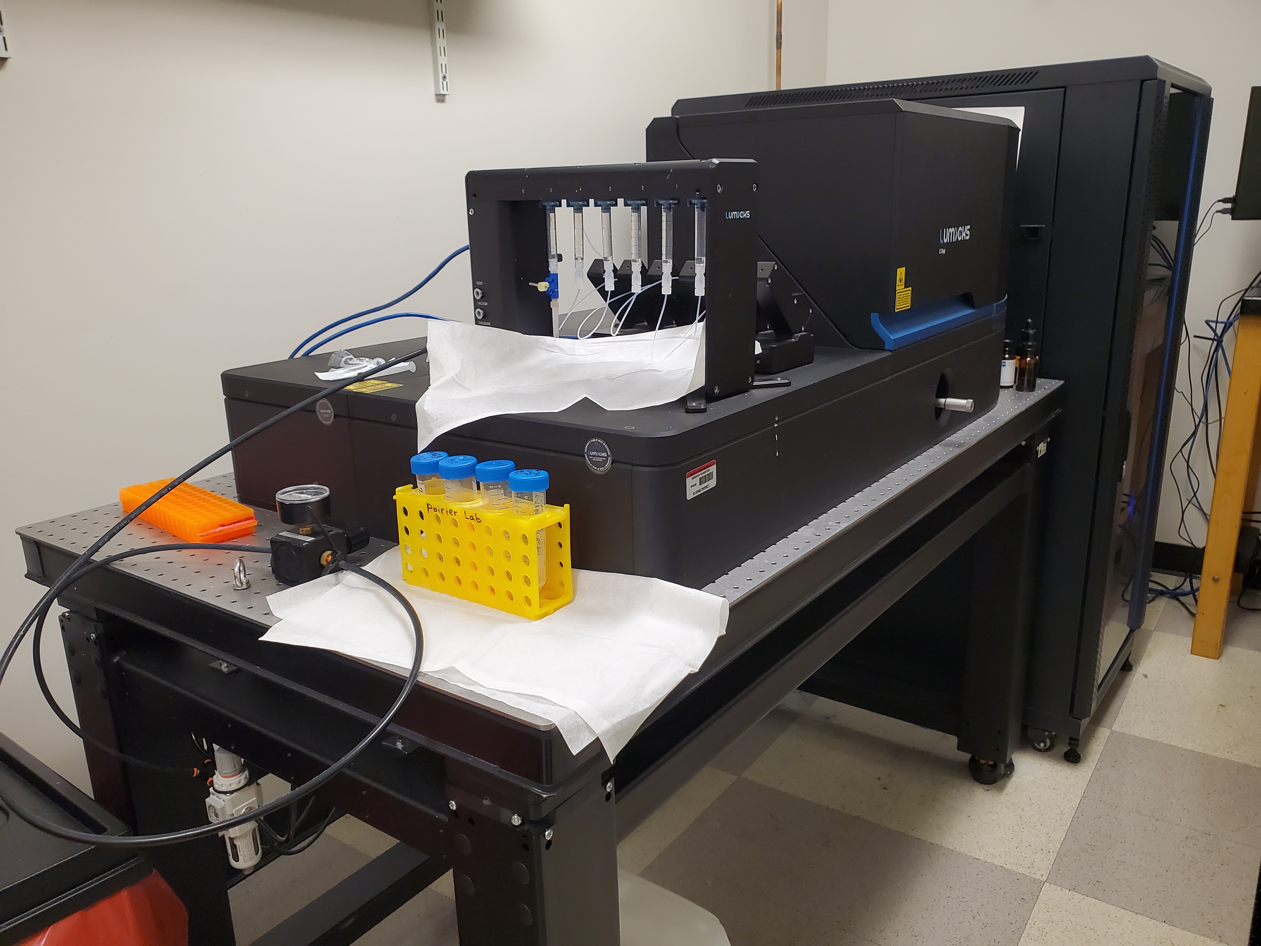
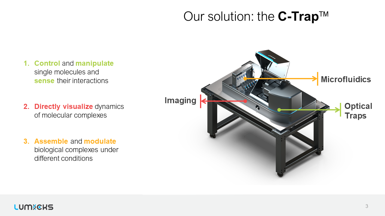
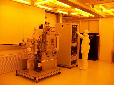
Located in PRB 0177C
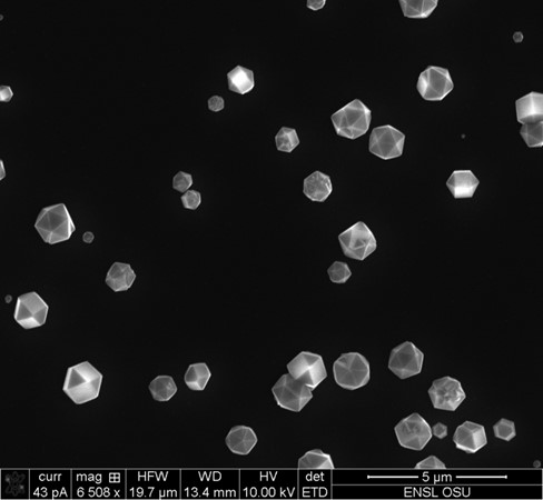
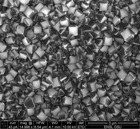
- Apreo 2S is a field emission gun (FEG) SEM with high performance, resolution, and contrast that combines advanced optics and detection with automation thus making obtaining high resolution imaging possible even for users new to SEM.
- Imaging resolution of 1.0 nm - 0.8 nm is achievable depending on the sample material, applied voltage (500 V - 30 kV) and working distance.
- Live quantitative SEM image coloring with ChemiSEM Technology is available based on energy dispersive X-ray spectroscopy (EDS). Point & ID, linescan, region, element maps are included.
- Low vacuum mode is available for imaging dielectrics with achievable 10 – 50 Pa water vapor chamber pressure.
- Multi-purpose sample holder is available. It hosts up to 18 standard stubs (Ø12 mm), three pre-tilted stubs, two pre-tilted row-bar holders (38° and 90°), a Faraday cup and does not require tools to mount a sample
- Electron channelling contrast imaging (ECCI) mode is available. ECCI is an electron diffraction technique enabling the study of defects in materials including dislocations or stacking faults that are close to the surface of the sample, low angle grain boundaries or atomic steps.
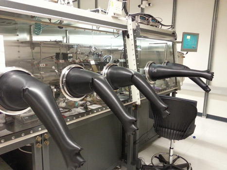
- CleanConnect Sample Transfer System, available on the instrument, enables quick sample transfer without exposing air-sensitive samples to atmosphere by maintaining inert gas or vacuum sample environment.
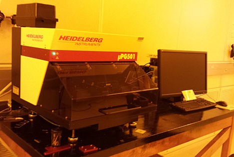
- The SEM is equipped with Nanometer Pattern Generation System (NPGS) v9.2 which is an SEM e-beal lithography system. NPGS uses QCAD, which is an open source CAD system, for pattern design.
|
 
|