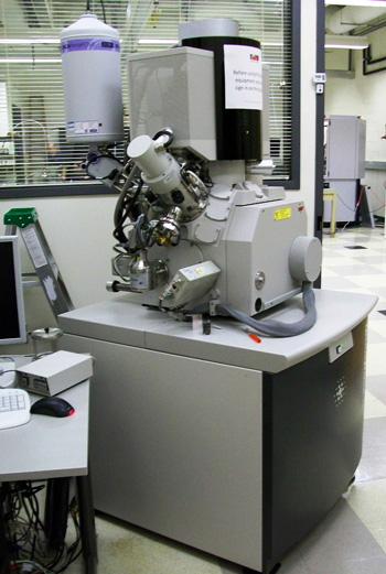
Located in PRB 0177C
- Sophisticated platform for sample preparation, imaging and analysis.
- Kleindeik Nanomanipulators for in situ electrical measurements and nanomanipulation
- Innovative Elstar electron column for high-resolution, high-contrast imaging
- High-performance Sidewinder ion column for fast, precise cross sectioning
- SEM imaging resolution as high as 0.9 nm at 15 kV at optimal working distance
- Additional capabilities: Pt deposition, X-ray EDS microanalysis, e-beam lithography
with Nabity NPGS software
Additional Capabilities include:
- Pt deposition
- X-ray EDS microanalysis with 2D material mapping
- e-beam lithography with Nabity NPGS software
- Two Kleindiek MM3A-EM nanomanipulator for in situ nanomanipulation and two-probe electrical measurements
Selected FIB/SEM applications:
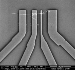
InP nanowire with Au contacts fabricated via e-beam
lithography.
From D. Ko,
L. Fang, F. Yang,
and E. Johnston-Halperin
|
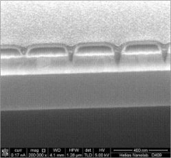
Pt capped ion beam cross
section of ion beam machined nanoholes in SiO2 layer.
From
S. Parks, and E. Johnston-Halperin
|
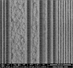
SEM image of SNAP wires
(Pt wires on Si). The second set of wires below the first set of wires can be seen.
From S. Parks, K. Li, and E. Johnston-Halperin
|
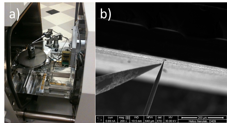
A) Kleindiek MM3A-EM nanomanipulator installed in the vacuum chamber of FIB/SEM.
B) Nanomanipultor probes in the close proximity of a sample surface.
From Dr. C. Marginean
|
|

